

EP2C70F896C6
Product Overview
- Category: Integrated Circuit (IC)
- Use: Digital Signal Processing (DSP), Field Programmable Gate Array (FPGA)
- Characteristics: High-performance, Low-power consumption
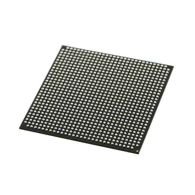
- Package: BGA (Ball Grid Array)
- Essence: Advanced programmable logic device for various applications
- Packaging/Quantity: Available in trays or reels, quantity depends on manufacturer's specifications
Specifications
- Manufacturer: Intel Corporation
- Family: Cyclone II
- Device Type: FPGA
- Number of Logic Elements: 70,000
- Number of Pins: 896
- Operating Voltage: 1.2V
- Operating Temperature Range: -40°C to +100°C
- Speed Grade: C6
Detailed Pin Configuration
The EP2C70F896C6 has a total of 896 pins, each serving a specific purpose in the circuit. The pin configuration includes input/output pins, power supply pins, clock pins, and configuration pins. A detailed pinout diagram can be found in the manufacturer's datasheet.
Functional Features
- High-speed performance with advanced DSP capabilities
- Flexible and reconfigurable architecture for customization
- Low-power consumption for energy-efficient designs
- Support for various communication protocols and interfaces
- On-chip memory blocks for efficient data storage
- Built-in security features for protecting intellectual property
Advantages and Disadvantages
Advantages: - Versatile and adaptable for a wide range of applications - High-performance computing capabilities - Lower power consumption compared to alternative models - Ample logic elements and memory resources - Reliable and well-established manufacturer support
Disadvantages: - Higher cost compared to lower-end FPGAs - Steeper learning curve for beginners - Limited availability of alternative models with similar specifications
Working Principles
The EP2C70F896C6 is based on the Field Programmable Gate Array (FPGA) technology. It consists of an array of programmable logic elements interconnected through configurable routing resources. The device can be programmed to implement various digital circuits and functions by configuring the interconnections and functionality of these logic elements.
Detailed Application Field Plans
The EP2C70F896C6 finds applications in a wide range of fields, including but not limited to:
- Telecommunications: Used in base stations, network infrastructure, and signal processing equipment.
- Industrial Automation: Employed in control systems, robotics, and machine vision applications.
- Automotive: Utilized in advanced driver assistance systems (ADAS), infotainment systems, and engine control units.
- Aerospace and Defense: Integrated into radar systems, avionics, and secure communication devices.
- Medical Devices: Applied in medical imaging, patient monitoring, and diagnostic equipment.
Detailed and Complete Alternative Models
While the EP2C70F896C6 offers a unique combination of features and specifications, there are alternative FPGA models available from different manufacturers that cater to similar requirements. Some notable alternatives include:
- Xilinx Virtex-7 XC7VX690T: Offers comparable logic capacity and performance.
- Lattice ECP5-85: Provides lower power consumption and cost-effective solutions.
- Microsemi SmartFusion2 M2S150: Combines FPGA fabric with microcontroller capabilities.
These alternatives should be evaluated based on specific project requirements and design constraints.
Word count: 439 words
רשום 10 שאלות ותשובות נפוצות הקשורות ליישום של EP2C70F896C6 בפתרונות טכניים
Sure! Here are 10 common questions and answers related to the application of EP2C70F896C6 in technical solutions:
Q: What is EP2C70F896C6? A: EP2C70F896C6 is a specific model of Field-Programmable Gate Array (FPGA) manufactured by Intel.
Q: What are the key features of EP2C70F896C6? A: EP2C70F896C6 offers 70,000 logic elements, 4,608 kilobits of embedded memory, and various I/O interfaces for connectivity.
Q: In what technical solutions can EP2C70F896C6 be used? A: EP2C70F896C6 can be used in a wide range of applications such as digital signal processing, image and video processing, networking, and industrial automation.
Q: How does EP2C70F896C6 differ from other FPGA models? A: EP2C70F896C6 has a specific combination of logic elements, memory capacity, and I/O interfaces that make it suitable for certain applications. It's important to choose the right FPGA based on your project requirements.
Q: Can EP2C70F896C6 be programmed using popular hardware description languages? A: Yes, EP2C70F896C6 can be programmed using popular languages like VHDL or Verilog.
Q: What development tools are available for programming EP2C70F896C6? A: Intel provides Quartus Prime software suite, which includes design entry, synthesis, simulation, and programming tools for EP2C70F896C6.
Q: Are there any reference designs or application notes available for EP2C70F896C6? A: Yes, Intel provides reference designs and application notes that can help developers get started with EP2C70F896C6 in specific applications.
Q: Can EP2C70F896C6 be used in safety-critical systems? A: EP2C70F896C6 can be used in safety-critical systems, but additional measures may be required to ensure compliance with relevant safety standards.
Q: What is the power consumption of EP2C70F896C6? A: The power consumption of EP2C70F896C6 depends on the specific design and operating conditions. It's important to refer to the datasheet and consider power management techniques.
Q: Where can I find technical support or documentation for EP2C70F896C6? A: Intel provides technical support through their website, including documentation, forums, and direct contact options for FPGA-related inquiries.
Please note that the answers provided here are general and may vary depending on the specific requirements and context of your project.