

5SGXEABK2H40I3N
Product Overview
- Category: Integrated Circuit (IC)
- Use: Digital Signal Processing
- Characteristics: High-performance, low-power consumption
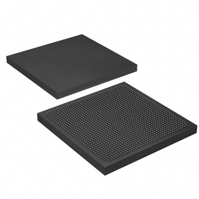
- Package: BGA (Ball Grid Array)
- Essence: FPGA (Field-Programmable Gate Array)
- Packaging/Quantity: Single unit
Specifications
- Manufacturer: Intel Corporation
- Technology: 5th Generation Stratix GXE
- Number of Logic Elements: 40,000
- Number of Embedded Multipliers: 2,400
- Operating Voltage: 1.2V
- Operating Temperature Range: -40°C to +100°C
- Package Dimensions: 40mm x 40mm
Detailed Pin Configuration
The 5SGXEABK2H40I3N has a total of 484 pins arranged in a ball grid array configuration. The pinout diagram and detailed pin descriptions can be found in the product datasheet provided by the manufacturer.
Functional Features
- High-speed digital signal processing capabilities
- Configurable logic elements for custom circuit implementation
- Embedded multipliers for efficient multiplication operations
- Low-power consumption design
- Support for various communication protocols
- On-chip memory resources for data storage
Advantages and Disadvantages
Advantages
- Versatile and flexible due to its field-programmable nature
- High-performance computing capabilities
- Lower development costs compared to custom ASICs (Application-Specific Integrated Circuits)
- Faster time-to-market for prototyping and product development
Disadvantages
- Limited resource availability compared to dedicated ASICs
- Higher power consumption compared to specialized processors
- Complexity in programming and configuring the FPGA
Working Principles
The 5SGXEABK2H40I3N is based on FPGA technology, which allows users to configure the device according to their specific requirements. The device consists of configurable logic elements, embedded multipliers, memory resources, and various I/O interfaces. Users can program the FPGA using hardware description languages (HDLs) or graphical tools to define the desired circuit functionality. Once programmed, the FPGA executes the configured circuit, enabling high-speed digital signal processing and other custom operations.
Detailed Application Field Plans
The 5SGXEABK2H40I3N finds applications in various fields, including:
- Telecommunications: Used in base stations, network routers, and switches for high-speed data processing.
- Industrial Automation: Employed in control systems, robotics, and machine vision applications for real-time processing and control.
- Medical Devices: Utilized in medical imaging equipment, patient monitoring systems, and diagnostic devices for data processing and analysis.
- Aerospace and Defense: Integrated into radar systems, communication satellites, and avionics for signal processing and encryption.
- Automotive: Applied in advanced driver-assistance systems (ADAS), infotainment systems, and engine control units (ECUs) for data processing and control.
Detailed and Complete Alternative Models
- Xilinx Virtex UltraScale+ VU9P: Offers higher logic capacity and performance.
- Altera Cyclone V E: Provides a cost-effective solution with lower resource availability.
- Lattice iCE40 UltraPlus: Suitable for low-power applications with limited logic requirements.
Please note that the above list is not exhaustive, and there are several alternative models available from different manufacturers.
Word count: 450 words
רשום 10 שאלות ותשובות נפוצות הקשורות ליישום של 5SGXEABK2H40I3N בפתרונות טכניים
Sure! Here are 10 common questions and answers related to the application of 5SGXEABK2H40I3N in technical solutions:
Q: What is the purpose of the 5SGXEABK2H40I3N FPGA? A: The 5SGXEABK2H40I3N FPGA is a Field-Programmable Gate Array designed for implementing complex digital logic circuits in various technical solutions.
Q: What are some typical applications of the 5SGXEABK2H40I3N FPGA? A: This FPGA can be used in applications such as high-performance computing, telecommunications, industrial automation, image processing, and data center acceleration.
Q: How does the 5SGXEABK2H40I3N FPGA differ from other FPGAs? A: The 5SGXEABK2H40I3N FPGA offers a unique combination of high-speed performance, low power consumption, and large capacity, making it suitable for demanding technical solutions.
Q: Can I reprogram the 5SGXEABK2H40I3N FPGA after it has been deployed in a solution? A: Yes, the 5SGXEABK2H40I3N FPGA is field-programmable, meaning you can reconfigure its functionality even after it has been integrated into a system.
Q: What tools are available for programming the 5SGXEABK2H40I3N FPGA? A: Intel Quartus Prime is the recommended software tool for designing, simulating, and programming the 5SGXEABK2H40I3N FPGA.
Q: How much logic capacity does the 5SGXEABK2H40I3N FPGA offer? A: The 5SGXEABK2H40I3N FPGA has a logic capacity of 40,000 equivalent LEs (Logic Elements), which can be used to implement various digital functions.
Q: What are the I/O capabilities of the 5SGXEABK2H40I3N FPGA? A: This FPGA offers a wide range of I/O options, including LVDS, differential signaling, single-ended signaling, and high-speed transceivers for data communication.
Q: Can the 5SGXEABK2H40I3N FPGA interface with other components or devices in a system? A: Yes, the FPGA supports various standard interfaces such as PCIe, Ethernet, USB, DDR memory, and SPI, allowing seamless integration with other system components.
Q: Is the 5SGXEABK2H40I3N FPGA suitable for real-time processing applications? A: Absolutely! With its high-speed performance and low-latency features, this FPGA is well-suited for real-time processing requirements in technical solutions.
Q: Are there any development boards available for prototyping with the 5SGXEABK2H40I3N FPGA? A: Yes, Intel provides development kits like the Arria V GX Starter Kit, which includes the 5SGXEABK2H40I3N FPGA, allowing developers to quickly prototype their designs.
Please note that the specific details and answers may vary depending on the context and requirements of the technical solution.