

5AGXBA5D6F31C6N
Product Overview
Category
The 5AGXBA5D6F31C6N belongs to the category of Field Programmable Gate Arrays (FPGAs).
Use
FPGAs are integrated circuits that can be programmed and reprogrammed to perform various digital functions. The 5AGXBA5D6F31C6N is specifically designed for applications requiring high-performance processing, such as telecommunications, industrial automation, and aerospace.
Characteristics
- High-performance FPGA with advanced features
- Large capacity for complex designs
- Low power consumption
- High-speed data processing capabilities
- Flexible and reconfigurable architecture
Package
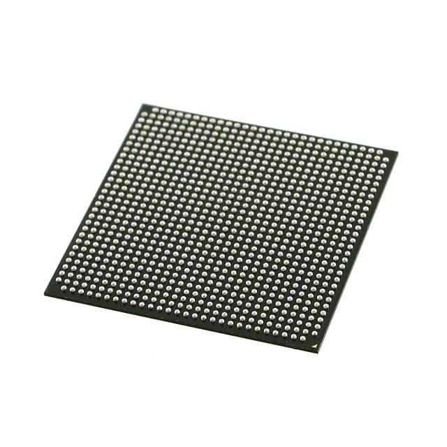
The 5AGXBA5D6F31C6N comes in a compact package suitable for surface mount technology (SMT) assembly. It is available in different package options, including ball grid array (BGA) and quad flat no-leads (QFN).
Essence
The essence of the 5AGXBA5D6F31C6N lies in its ability to provide a versatile and powerful platform for implementing complex digital systems. Its programmable nature allows for customization and adaptability to specific application requirements.
Packaging/Quantity
The 5AGXBA5D6F31C6N is typically sold in reels or trays, depending on the chosen package type. The quantity per reel or tray may vary, but it is commonly available in quantities suitable for both prototyping and production purposes.
Specifications
- Logic Elements: 5,200,000
- Embedded Memory: Up to 10,368 Kbits
- DSP Blocks: 3,840
- Maximum User I/Os: 1,080
- Clock Networks: Up to 16 global clocks
- Operating Voltage: 1.2V
- Operating Temperature: -40°C to 100°C
- Package Options: BGA, QFN
Detailed Pin Configuration
The pin configuration of the 5AGXBA5D6F31C6N varies depending on the chosen package type. Please refer to the manufacturer's datasheet for the specific pinout details.
Functional Features
- High-speed data processing: The 5AGXBA5D6F31C6N offers high-performance capabilities, enabling rapid data processing and efficient execution of complex algorithms.
- Reconfigurability: The FPGA can be reprogrammed to adapt to changing requirements or to implement different functionalities without the need for hardware changes.
- Embedded memory: The device includes a significant amount of embedded memory, allowing for efficient storage and retrieval of data within the FPGA itself.
- DSP blocks: Dedicated digital signal processing (DSP) blocks provide enhanced capabilities for applications requiring real-time signal processing.
- Flexible I/O options: The FPGA supports a large number of user I/Os, facilitating seamless integration with external devices and systems.
Advantages and Disadvantages
Advantages
- Versatility: The 5AGXBA5D6F31C6N can be used in a wide range of applications due to its programmable nature.
- High performance: The FPGA offers powerful processing capabilities, making it suitable for demanding tasks.
- Power efficiency: The low power consumption of the device helps reduce energy costs and extends battery life in portable applications.
- Scalability: The FPGA's large capacity allows for the implementation of complex designs and future expansion.
Disadvantages
- Complexity: Programming and configuring FPGAs require specialized knowledge and expertise.
- Cost: FPGAs can be more expensive compared to other integrated circuits due to their advanced features and flexibility.
- Time-consuming development: Designing and optimizing FPGA-based systems may require significant development time and resources.
Working Principles
The 5AGXBA5D6F31C6N operates based on the principles of reconfigurable logic. It consists of an array of programmable logic elements interconnected through configurable routing resources. The device can be programmed using hardware description languages (HDLs) or graphical tools to define the desired functionality. Upon configuration, the FPGA executes the programmed logic, enabling the implementation of complex digital systems.
Detailed Application Field Plans
The 5AGXBA5D6F31C6N finds applications in various fields, including:
- Telecommunications: The FPGA's high-speed processing capabilities make it suitable for implementing communication protocols, signal processing algorithms, and network infrastructure.
- Industrial Automation: The device can be used in industrial control systems, robotics, and machine vision applications, providing real-time processing and flexibility for adapting to changing requirements.
- Aerospace: FPGAs are utilized in aerospace applications for tasks such as radar signal processing, image and video processing, and flight control systems.
Detailed and Complete Alternative Models
- 5AGXBA7D4F31
רשום 10 שאלות ותשובות נפוצות הקשורות ליישום של 5AGXBA5D6F31C6N בפתרונות טכניים
Sure! Here are 10 common questions and answers related to the application of 5AGXBA5D6F31C6N in technical solutions:
Q: What is the 5AGXBA5D6F31C6N FPGA used for? A: The 5AGXBA5D6F31C6N FPGA is a field-programmable gate array that can be used for various applications, including digital signal processing, high-performance computing, and embedded systems.
Q: What are the key features of the 5AGXBA5D6F31C6N FPGA? A: Some key features of this FPGA include a large number of logic elements, high-speed transceivers, embedded memory blocks, and support for various communication protocols.
Q: How can I program the 5AGXBA5D6F31C6N FPGA? A: The 5AGXBA5D6F31C6N FPGA can be programmed using hardware description languages (HDLs) such as VHDL or Verilog, or through graphical programming tools like Quartus Prime.
Q: Can the 5AGXBA5D6F31C6N FPGA be used for real-time image processing? A: Yes, the 5AGXBA5D6F31C6N FPGA can be utilized for real-time image processing tasks due to its high computational power and parallel processing capabilities.
Q: Is the 5AGXBA5D6F31C6N FPGA suitable for implementing cryptographic algorithms? A: Absolutely, the 5AGXBA5D6F31C6N FPGA can be effectively used for implementing cryptographic algorithms due to its ability to handle complex computations and secure data processing.
Q: Can the 5AGXBA5D6F31C6N FPGA interface with external devices? A: Yes, the 5AGXBA5D6F31C6N FPGA supports various communication protocols like PCIe, Ethernet, USB, and I2C, allowing it to interface with a wide range of external devices.
Q: What is the power consumption of the 5AGXBA5D6F31C6N FPGA? A: The power consumption of the 5AGXBA5D6F31C6N FPGA depends on the specific design and usage scenario. It is recommended to refer to the datasheet for detailed power specifications.
Q: Can the 5AGXBA5D6F31C6N FPGA be reprogrammed multiple times? A: Yes, the 5AGXBA5D6F31C6N FPGA is a reprogrammable device, allowing you to modify and update the configuration multiple times as per your requirements.
Q: Are there any development boards available for the 5AGXBA5D6F31C6N FPGA? A: Yes, Intel (formerly Altera) provides development boards like the Arria V GX Starter Kit that feature the 5AGXBA5D6F31C6N FPGA, enabling easy prototyping and development.
Q: Where can I find documentation and resources for the 5AGXBA5D6F31C6N FPGA? A: You can find documentation, datasheets, reference designs, and other resources for the 5AGXBA5D6F31C6N FPGA on the official Intel (formerly Altera) website or their support portal.
Please note that the specific details and answers may vary depending on the context and requirements of your technical solution.