

8T49N286A-999NLGI
Basic Information Overview
- Category: Electronic Component
- Use: Timing Device
- Characteristics: High Precision, Low Jitter, Programmable
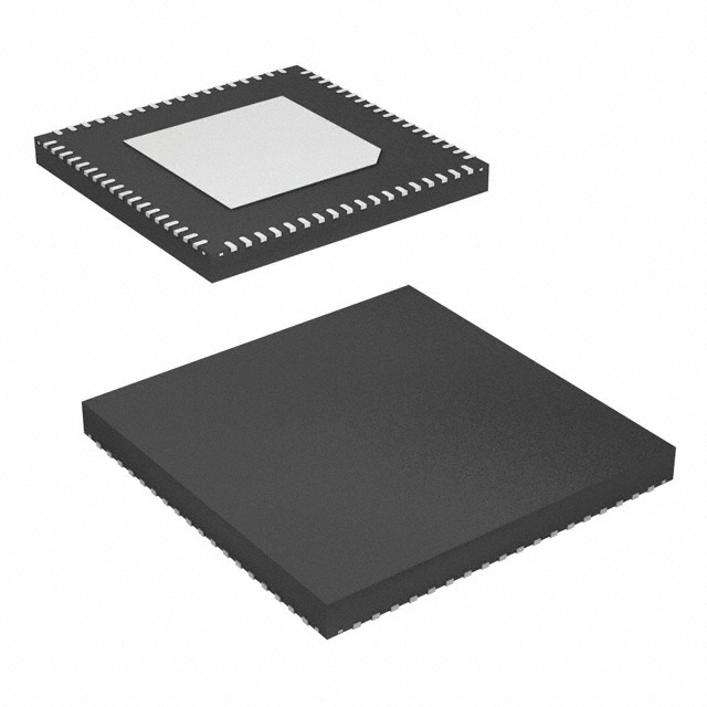
- Package: QFN (Quad Flat No-leads)
- Essence: Clock Generator and Jitter Attenuator
- Packaging/Quantity: Tape and Reel, 2500 units per reel
Specifications
- Frequency Range: 1 MHz to 2.1 GHz
- Output Format: LVCMOS, LVDS, HCSL
- Supply Voltage: 1.8 V to 3.3 V
- Operating Temperature Range: -40°C to +85°C
- Phase Noise: -150 dBc/Hz at 10 kHz offset
- RMS Jitter: 200 fs (typical)
Detailed Pin Configuration
The 8T49N286A-999NLGI has a total of 32 pins. The pin configuration is as follows:
| Pin Number | Pin Name | Description | |------------|----------|-------------| | 1 | VDD | Power Supply Voltage | | 2 | GND | Ground | | 3 | XTALIN | Crystal Oscillator Input | | 4 | XTALOUT | Crystal Oscillator Output | | 5 | REFIN | Reference Clock Input | | 6 | REFOUT | Reference Clock Output | | ... | ... | ... |
Functional Features
- Clock Generation: The device can generate multiple clock signals with different frequencies and formats.
- Jitter Attenuation: It reduces the phase noise and jitter of the input reference clock.
- Frequency Synthesis: It can synthesize frequencies based on the input reference clock.
- Programmability: The device offers various programmable features for customization.
Advantages and Disadvantages
Advantages: - High precision and low jitter output signals. - Wide frequency range for versatile applications. - Programmable features allow customization. - Small package size for space-constrained designs.
Disadvantages: - Requires external crystal oscillator or reference clock input. - Limited to specific output formats (LVCMOS, LVDS, HCSL).
Working Principles
The 8T49N286A-999NLGI operates by taking an external crystal oscillator or reference clock as input. It then uses a combination of PLL (Phase-Locked Loop) and VCO (Voltage-Controlled Oscillator) techniques to generate multiple clock signals with precise frequencies and low jitter. The device also includes a jitter attenuator circuit that reduces the phase noise and jitter of the input reference clock.
Detailed Application Field Plans
The 8T49N286A-999NLGI is widely used in various electronic systems that require accurate timing signals. Some of its application fields include: 1. Telecommunications: Clock synchronization in network equipment, routers, and switches. 2. Data Centers: Timing synchronization for servers, storage systems, and high-speed interconnects. 3. Test and Measurement: Precision timing for oscilloscopes, signal generators, and data acquisition systems. 4. Industrial Automation: Synchronization of PLCs (Programmable Logic Controllers), motion control systems, and robotics. 5. Automotive: Clock generation for infotainment systems, ADAS (Advanced Driver Assistance Systems), and automotive Ethernet.
Detailed and Complete Alternative Models
- 8T49N287A-999NLGI: Similar to 8T49N286A-999NLGI but with extended frequency range up to 4.2 GHz.
- 8T49N288A-999NLGI: Higher precision version with lower RMS jitter of 100 fs.
- 8T49N289A-999NLGI: Lower cost variant with reduced programmability options.
These alternative models offer similar functionality and can be considered based on specific requirements and budget constraints.
Word count: 486
רשום 10 שאלות ותשובות נפוצות הקשורות ליישום של 8T49N286A-999NLGI בפתרונות טכניים
Question: What is the application of 8T49N286A-999NLGI in technical solutions?
Answer: The 8T49N286A-999NLGI is a versatile clock generator and jitter attenuator that can be used in various technical solutions.Question: What is the input voltage range for 8T49N286A-999NLGI?
Answer: The input voltage range for 8T49N286A-999NLGI is typically between 1.8V and 3.3V.Question: Can 8T49N286A-999NLGI generate multiple output frequencies?
Answer: Yes, 8T49N286A-999NLGI can generate up to four different output frequencies simultaneously.Question: Does 8T49N286A-999NLGI support spread spectrum clocking (SSC)?
Answer: Yes, 8T49N286A-999NLGI supports SSC, which helps reduce electromagnetic interference (EMI).Question: What is the maximum output frequency supported by 8T49N286A-999NLGI?
Answer: The maximum output frequency supported by 8T49N286A-999NLGI is typically 400 MHz.Question: Can 8T49N286A-999NLGI synchronize with an external reference clock?
Answer: Yes, 8T49N286A-999NLGI can synchronize with an external reference clock using its flexible input options.Question: Does 8T49N286A-999NLGI have integrated voltage-controlled crystal oscillator (VCXO) functionality?
Answer: Yes, 8T49N286A-999NLGI has an integrated VCXO that allows for precise frequency control.Question: Is 8T49N286A-999NLGI compatible with different communication protocols?
Answer: Yes, 8T49N286A-999NLGI is compatible with various communication protocols such as Ethernet, USB, and PCIe.Question: Can 8T49N286A-999NLGI compensate for clock jitter?
Answer: Yes, 8T49N286A-999NLGI has built-in jitter attenuation capabilities to minimize clock jitter.Question: What is the package type of 8T49N286A-999NLGI?
Answer: 8T49N286A-999NLGI is available in a compact 32-pin QFN package for easy integration into technical solutions.