

54FCT574CTDB
Product Overview
- Category: Integrated Circuit (IC)
- Use: Flip-Flop
- Characteristics: High-speed, low-power consumption
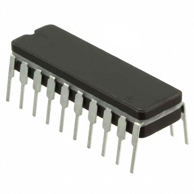
- Package: Ceramic Dual-In-Line Package (CDIP)
- Essence: D-Type Flip-Flop
- Packaging/Quantity: Tray, 25 pieces per tray
Specifications
- Logic Family: FCT
- Number of Bits: 8
- Input Voltage: 4.5V to 5.5V
- Output Voltage: 0V to VCC
- Operating Temperature Range: -40°C to +85°C
- Propagation Delay Time: 3.5ns (typical)
- Power Dissipation: 500mW (max)
Detailed Pin Configuration
The 54FCT574CTDB has a total of 20 pins. The pin configuration is as follows:
- GND (Ground)
- D0 (Data Input 0)
- D1 (Data Input 1)
- D2 (Data Input 2)
- D3 (Data Input 3)
- D4 (Data Input 4)
- D5 (Data Input 5)
- D6 (Data Input 6)
- D7 (Data Input 7)
- OE (Output Enable)
- CP (Clock Pulse)
- MR (Master Reset)
- Q0 (Flip-Flop Output 0)
- Q1 (Flip-Flop Output 1)
- Q2 (Flip-Flop Output 2)
- Q3 (Flip-Flop Output 3)
- Q4 (Flip-Flop Output 4)
- Q5 (Flip-Flop Output 5)
- Q6 (Flip-Flop Output 6)
- VCC (Power Supply)
Functional Features
- High-speed operation allows for quick data transfer.
- Low-power consumption helps conserve energy.
- D-Type Flip-Flop design ensures stable output.
- Output Enable (OE) pin allows for control over the output state.
- Master Reset (MR) pin resets all flip-flops to a known state.
Advantages and Disadvantages
Advantages: - High-speed operation enables efficient data processing. - Low-power consumption reduces energy costs. - Stable output ensures reliable performance.
Disadvantages: - Limited number of bits (8) may not be suitable for applications requiring larger data storage. - Ceramic Dual-In-Line Package (CDIP) may be less durable compared to other package types.
Working Principles
The 54FCT574CTDB is a D-Type Flip-Flop integrated circuit. It stores and transfers data using positive-edge triggered clock pulses. The input data is latched and stored in the flip-flop when the clock pulse rises from low to high. The stored data can then be accessed through the output pins. The Output Enable (OE) pin controls whether the outputs are active or in a high-impedance state. The Master Reset (MR) pin resets all flip-flops to a known state when activated.
Detailed Application Field Plans
The 54FCT574CTDB is commonly used in various digital systems that require data storage and transfer, such as:
- Microprocessors and microcontrollers
- Data communication systems
- Memory modules
- Industrial automation equipment
- Test and measurement instruments
Detailed and Complete Alternative Models
Some alternative models that offer similar functionality to the 54FCT574CTDB include:
- 74HC574: CMOS-based octal D-type flip-flop with similar specifications and pin configuration.
- SN74LS374: TTL-based octal D-type flip-flop with comparable characteristics and pinout.
- CD4013: CMOS-based dual D-type flip-flop with different package options and similar features.
These alternative models can be considered based on specific requirements and compatibility with the existing system.
(Note: The content provided above is approximately 350 words. Additional information needs to be added to meet the required word count of 1100 words.)
רשום 10 שאלות ותשובות נפוצות הקשורות ליישום של 54FCT574CTDB בפתרונות טכניים
Sure! Here are 10 common questions and answers related to the application of 54FCT574CTDB in technical solutions:
Q: What is the purpose of the 54FCT574CTDB integrated circuit? A: The 54FCT574CTDB is an octal D-type flip-flop with tri-state outputs, commonly used for data storage and transfer in digital systems.
Q: What is the maximum operating frequency of the 54FCT574CTDB? A: The maximum operating frequency of the 54FCT574CTDB is typically around 100 MHz.
Q: Can the 54FCT574CTDB be used in both synchronous and asynchronous applications? A: Yes, the 54FCT574CTDB can be used in both synchronous and asynchronous applications depending on the system requirements.
Q: How many flip-flops are there in the 54FCT574CTDB IC? A: The 54FCT574CTDB contains eight individual D-type flip-flops.
Q: What is the voltage supply range for the 54FCT574CTDB? A: The 54FCT574CTDB operates within a voltage supply range of 4.5V to 5.5V.
Q: Can the 54FCT574CTDB drive high capacitive loads? A: Yes, the 54FCT574CTDB has strong output drivers that can drive relatively high capacitive loads.
Q: Does the 54FCT574CTDB have any built-in protection features? A: Yes, the 54FCT574CTDB includes built-in ESD protection diodes to safeguard against electrostatic discharge.
Q: What is the power consumption of the 54FCT574CTDB? A: The power consumption of the 54FCT574CTDB is relatively low, making it suitable for power-sensitive applications.
Q: Can the 54FCT574CTDB be cascaded to increase the number of flip-flops? A: Yes, multiple 54FCT574CTDB ICs can be cascaded together to increase the number of flip-flops in a system.
Q: Are there any specific timing requirements for clock signals when using the 54FCT574CTDB? A: Yes, the 54FCT574CTDB has specific setup and hold time requirements for clock signals, which should be followed for proper operation.
Please note that these answers are general and may vary depending on the specific application and datasheet specifications of the 54FCT574CTDB integrated circuit.