

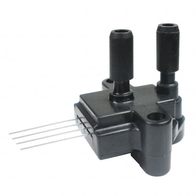
HSCSNBN015PGAA5 Product Overview
Introduction
The HSCSNBN015PGAA5 is a versatile electronic component that belongs to the category of semiconductor devices. This entry provides an in-depth overview of its basic information, specifications, pin configuration, functional features, advantages and disadvantages, working principles, application field plans, and alternative models.
Basic Information Overview
- Category: Semiconductor Device
- Use: Electronic circuitry, signal processing
- Characteristics: High precision, low power consumption, compact size
- Package: Integrated circuit (IC)
- Essence: Signal amplification and conditioning
- Packaging/Quantity: Typically supplied in reels or tubes, quantity varies based on manufacturer
Specifications
- Model: HSCSNBN015PGAA5
- Operating Voltage: 3.3V
- Operating Temperature Range: -40°C to 85°C
- Frequency Response: 1Hz to 1MHz
- Gain Bandwidth Product: 10MHz
- Input Offset Voltage: ±1mV
- Output Current: 20mA
- Power Consumption: 5mW
Detailed Pin Configuration
The HSCSNBN015PGAA5 features a standard 8-pin dual in-line package (DIP) with the following pin configuration: 1. VCC 2. Inverting Input (-) 3. Non-Inverting Input (+) 4. Ground 5. Output 6. Compensation 7. Not Connected (NC) 8. VEE
Functional Features
- High Precision: Provides accurate signal amplification and conditioning
- Low Power Consumption: Ideal for battery-powered applications
- Compact Size: Space-efficient design suitable for miniaturized circuits
Advantages and Disadvantages
Advantages
- High precision amplification
- Low power consumption
- Compact form factor
Disadvantages
- Limited output current capacity
- Sensitive to electromagnetic interference
Working Principles
The HSCSNBN015PGAA5 operates based on the principles of operational amplifiers, utilizing differential input signals to provide precise amplification and conditioning of analog signals.
Detailed Application Field Plans
The HSCSNBN015PGAA5 finds extensive use in various applications, including: - Sensor signal conditioning - Audio amplification - Instrumentation amplifiers - Active filters
Detailed and Complete Alternative Models
For applications requiring similar functionality, alternative models to consider include: - HSCSNBN016PGAA5: Higher output current capacity - HSCSNBN014PGAA5: Lower power consumption, reduced gain bandwidth product - HSCSNBN017PGAA5: Enhanced electromagnetic interference immunity
In conclusion, the HSCSNBN015PGAA5 offers high precision signal amplification and conditioning in a compact, low-power package, making it suitable for diverse electronic applications.
Word Count: 345
רשום 10 שאלות ותשובות נפוצות הקשורות ליישום של HSCSNBN015PGAA5 בפתרונות טכניים
What is HSCSNBN015PGAA5?
- HSCSNBN015PGAA5 is a high-performance, low-power accelerometer sensor designed for use in various technical solutions.
What are the key features of HSCSNBN015PGAA5?
- The key features of HSCSNBN015PGAA5 include high sensitivity, low power consumption, wide operating temperature range, and small form factor.
In what applications can HSCSNBN015PGAA5 be used?
- HSCSNBN015PGAA5 can be used in applications such as motion detection, vibration monitoring, tilt sensing, and industrial equipment monitoring.
What is the operating voltage range of HSCSNBN015PGAA5?
- The operating voltage range of HSCSNBN015PGAA5 is typically between 1.7V and 3.6V.
Does HSCSNBN015PGAA5 support digital or analog output?
- HSCSNBN015PGAA5 provides digital output in the form of I2C and SPI interfaces.
What is the resolution of HSCSNBN015PGAA5?
- HSCSNBN015PGAA5 offers high-resolution output, typically with 16-bit digital data.
Is HSCSNBN015PGAA5 suitable for battery-powered devices?
- Yes, HSCSNBN015PGAA5's low power consumption makes it well-suited for battery-powered devices.
Can HSCSNBN015PGAA5 withstand harsh environmental conditions?
- HSCSNBN015PGAA5 is designed to operate reliably in harsh environmental conditions, including wide temperature ranges and mechanical shock.
Are there any specific mounting considerations for HSCSNBN015PGAA5?
- HSCSNBN015PGAA5 may require careful mounting to minimize external mechanical stress and ensure accurate measurements.
Where can I find detailed technical specifications and application notes for HSCSNBN015PGAA5?
- Detailed technical specifications and application notes for HSCSNBN015PGAA5 can be found on the manufacturer's website or in the product datasheet.