

PI49FCT807TQEX
Overview
Category
The PI49FCT807TQEX belongs to the category of integrated circuits (ICs).
Use
It is commonly used in electronic devices for signal transmission and processing.
Characteristics
- High-speed operation
- Low power consumption
- Compact package size
- Wide operating voltage range
Package
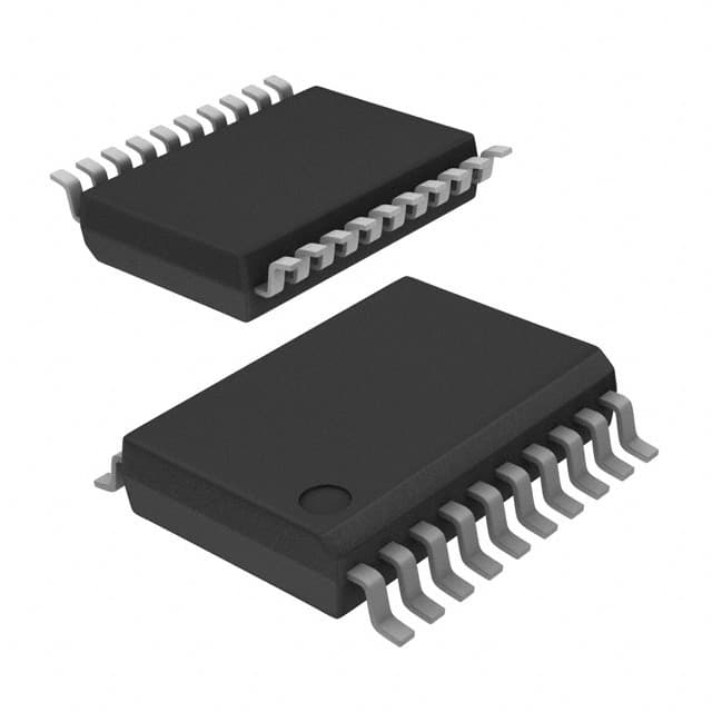
The PI49FCT807TQEX is available in a small outline integrated circuit (SOIC) package.
Essence
This IC is designed to provide reliable and efficient signal transmission within electronic systems.
Packaging/Quantity
The PI49FCT807TQEX is typically packaged in reels or tubes, with a quantity of 250 units per reel/tube.
Specifications and Parameters
- Operating Voltage: 2.5V - 5.5V
- Input Voltage Range: 0V - VCC
- Output Voltage Range: 0V - VCC
- Operating Temperature Range: -40°C to +85°C
- Input Capacitance: 4pF (typical)
- Output Capacitance: 6pF (typical)
- Propagation Delay: 3.5ns (typical)
- Output Skew: 200ps (typical)
Pin Configuration
The PI49FCT807TQEX features a total of 16 pins, arranged as follows:
1   GND
2   A0
3   A1
4   A2
5   A3
6   A4
7   A5
8   A6
9   A7
10  OE#
11  Y0
12  Y1
13  Y2
14  Y3
15  VCC
16  GND
Functional Characteristics
The PI49FCT807TQEX is a high-speed octal buffer/line driver with 3-state outputs. It provides non-inverting buffers and features an output enable control (OE#) pin for easy control of the output state.
Advantages and Disadvantages
Advantages
- High-speed operation allows for efficient signal transmission.
- Low power consumption helps to conserve energy.
- Compact package size enables space-saving designs.
- Wide operating voltage range ensures compatibility with various systems.
Disadvantages
- Limited number of output pins (8) may not be sufficient for certain applications.
- May require additional external components for specific circuit configurations.
Applicable Range of Products
The PI49FCT807TQEX is suitable for use in a wide range of electronic devices, including but not limited to: - Computers and laptops - Telecommunications equipment - Consumer electronics - Industrial automation systems - Automotive electronics
Working Principles
The PI49FCT807TQEX operates by receiving input signals and amplifying them to drive corresponding output lines. The output enable control (OE#) pin allows for easy control of the output state, enabling or disabling the transmission of signals.
Detailed Application Field Plans
The PI49FCT807TQEX can be applied in various fields, such as: 1. Data communication systems: Used for signal buffering and line driving in high-speed data transmission. 2. Memory modules: Enables efficient signal transmission between memory chips and other components. 3. Display systems: Facilitates the driving of display panels, ensuring accurate and reliable image rendering. 4. Networking equipment: Enhances signal integrity in networking devices, improving overall performance. 5. Industrial control systems: Provides reliable signal transmission in control systems, ensuring precise operation.
Detailed Alternative Models
Some alternative models to the PI49FCT807TQEX include: - PI74FCT807TQEX - PI49FCT807TQEXX - PI49FCT807TQEXY - PI49FCT807TQEXZ
5 Common Technical Questions and Answers
Q: What is the maximum operating voltage for the PI49FCT807TQEX? A: The maximum operating voltage is 5.5V.
Q: Can I use this IC in automotive applications? A: Yes, the PI49FCT807TQEX is suitable for automotive electronics.
Q: What is the typical propagation delay of this IC? A: The typical propagation delay is 3.5ns.
Q: How many output pins does the PI49FCT807TQEX have? A: It has a total of 8 output pins.
Q: Is the PI49FCT807TQEX compatible with 3.3V systems? A: Yes, it can operate within a voltage range of 2.5V to 5.5V, making it compatible with 3.3V systems.
This