

Encyclopedia Entry: 74LVC374AQ20-13
Product Overview
Category
The 74LVC374AQ20-13 belongs to the category of integrated circuits (ICs).
Use
This IC is commonly used in digital electronics for various applications such as data storage, signal buffering, and data transfer.
Characteristics
- Low-voltage CMOS technology
- High-speed operation
- Wide operating voltage range
- Schmitt-trigger action on all inputs
- 3-state outputs
- Power-down protection
- ESD protection
Package
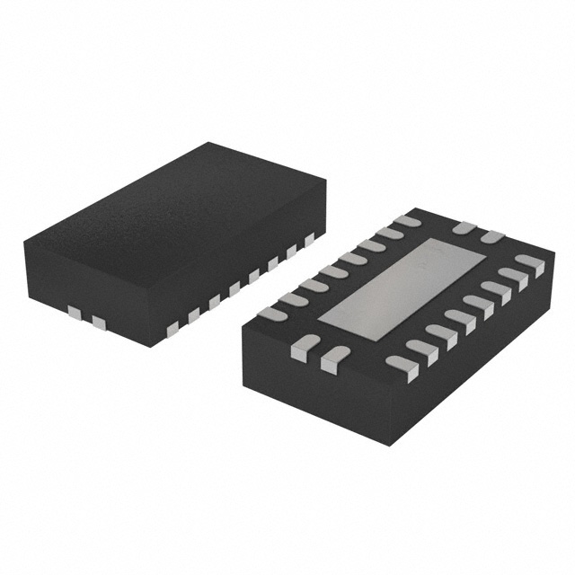
The 74LVC374AQ20-13 is available in a 20-pin TSSOP (Thin Shrink Small Outline Package) package.
Essence
The essence of the 74LVC374AQ20-13 lies in its ability to store and manipulate digital data efficiently, providing reliable signal buffering and transfer capabilities.
Packaging/Quantity
This IC is typically packaged in reels or tubes, with a quantity of 2500 units per reel/tube.
Specifications
- Supply Voltage Range: 1.65V to 5.5V
- Input Voltage Range: -0.5V to VCC + 0.5V
- Output Voltage Range: 0V to VCC
- Operating Temperature Range: -40°C to +125°C
- Maximum Clock Frequency: 100 MHz
Detailed Pin Configuration
The 74LVC374AQ20-13 has a total of 20 pins, each serving a specific function. The pin configuration is as follows:
- Pin 1: Data Input D0
- Pin 2: Data Input D1
- Pin 3: Data Input D2
- Pin 4: Data Input D3
- Pin 5: Data Input D4
- Pin 6: Data Input D5
- Pin 7: Data Input D6
- Pin 8: Data Input D7
- Pin 9: Clock Input CP
- Pin 10: Output Enable Input OE
- Pin 11: Master Reset Input MR
- Pin 12: Q0 Output
- Pin 13: Q1 Output
- Pin 14: Q2 Output
- Pin 15: Q3 Output
- Pin 16: Q4 Output
- Pin 17: Q5 Output
- Pin 18: Q6 Output
- Pin 19: Q7 Output
- Pin 20: Ground (GND)
Functional Features
The 74LVC374AQ20-13 offers the following functional features:
- Data storage and transfer: The IC can store data on its inputs and transfer it to the outputs when triggered by the clock input.
- Signal buffering: It provides buffering capabilities to ensure reliable signal transmission between different components of a digital circuit.
- 3-state outputs: The outputs can be put into a high-impedance state, allowing multiple devices to share the same bus without interference.
- Power-down protection: The IC has built-in protection mechanisms to prevent damage during power-down situations.
- ESD protection: It incorporates measures to protect against electrostatic discharge, enhancing its durability.
Advantages and Disadvantages
Advantages
- High-speed operation enables efficient data processing.
- Wide operating voltage range allows compatibility with various systems.
- Schmitt-trigger action on all inputs ensures reliable signal detection.
- 3-state outputs facilitate bus sharing in complex circuits.
- Power-down and ESD protection enhance reliability.
Disadvantages
- Limited maximum clock frequency may restrict its use in high-speed applications.
- Availability in only one package type may limit integration options.
Working Principles
The 74LVC374AQ20-13 operates based on the principles of digital logic. It utilizes flip-flops to store data and a clock input to control the transfer of data from inputs to outputs. The IC's internal circuitry ensures reliable signal detection, buffering, and protection against power-down situations and electrostatic discharge.
Detailed Application Field Plans
The 74LVC374AQ20-13 finds applications in various fields, including:
- Microcontrollers: Used for interfacing with external devices and storing temporary data.
- Communication systems: Facilitates data buffering and transfer between different components.
- Data storage systems: Enables efficient data storage and retrieval operations.
- Industrial automation: Provides reliable signal buffering and transfer capabilities in control systems.
- Automotive electronics: Used for data processing and signal conditioning in automotive applications.
Detailed and Complete Alternative Models
- 74HC374: Similar functionality but operates at higher voltages (2V to 6V).
- SN74LVCH374A: Offers similar features with a wider operating temperature range (-55°C to +125°C). 3
רשום 10 שאלות ותשובות נפוצות הקשורות ליישום של 74LVC374AQ20-13 בפתרונות טכניים
Sure! Here are 10 common questions and answers related to the application of 74LVC374AQ20-13 in technical solutions:
Q: What is the function of the 74LVC374AQ20-13? A: The 74LVC374AQ20-13 is an octal D-type flip-flop with 3-state outputs. It can store and transfer data in digital circuits.
Q: What is the operating voltage range for the 74LVC374AQ20-13? A: The 74LVC374AQ20-13 operates within a voltage range of 1.65V to 5.5V.
Q: How many flip-flops are there in the 74LVC374AQ20-13? A: The 74LVC374AQ20-13 has 8 flip-flops, making it an octal (8-bit) device.
Q: What is the maximum clock frequency supported by the 74LVC374AQ20-13? A: The 74LVC374AQ20-13 can operate at a maximum clock frequency of 133 MHz.
Q: Can the 74LVC374AQ20-13 be used in both parallel and serial data transfer applications? A: Yes, the 74LVC374AQ20-13 supports both parallel and serial data transfer modes.
Q: Does the 74LVC374AQ20-13 have any built-in output enable functionality? A: Yes, the 74LVC374AQ20-13 has an active-low output enable (OE) pin that can be used to disable the outputs.
Q: What is the power supply current consumption of the 74LVC374AQ20-13? A: The power supply current consumption of the 74LVC374AQ20-13 depends on the operating conditions, but typically ranges from a few microamps to a few milliamps.
Q: Can the 74LVC374AQ20-13 be cascaded to increase the number of flip-flops? A: Yes, multiple 74LVC374AQ20-13 devices can be cascaded together to increase the number of flip-flops in a circuit.
Q: What is the output drive strength of the 74LVC374AQ20-13? A: The 74LVC374AQ20-13 has a typical output drive strength of ±24 mA.
Q: Is the 74LVC374AQ20-13 compatible with other logic families? A: Yes, the 74LVC374AQ20-13 is designed to be compatible with both TTL and CMOS logic families, making it versatile for various applications.
Please note that these answers are general and may vary depending on the specific datasheet and application requirements.