

74LVC1G07FS3-7
Product Overview
Category
The 74LVC1G07FS3-7 belongs to the category of integrated circuits (ICs).
Use
This IC is commonly used as a buffer/driver for various digital signals.
Characteristics
- Low voltage CMOS technology
- High-speed operation
- Wide operating voltage range
- Schmitt-trigger input
- Open-drain output
- Small package size
Package
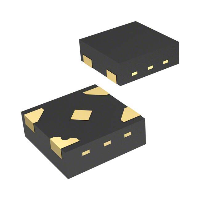
The 74LVC1G07FS3-7 is available in a small SOT-353 package.
Essence
The essence of this product lies in its ability to provide buffering and driving capabilities for digital signals, ensuring reliable signal transmission.
Packaging/Quantity
The 74LVC1G07FS3-7 is typically packaged in reels or tubes, with a quantity of 3000 units per reel/tube.
Specifications
- Supply Voltage Range: 1.65V to 5.5V
- Input Voltage Range: 0V to VCC
- Output Voltage Range: 0V to VCC
- Maximum Operating Frequency: 500 MHz
- Maximum Propagation Delay: 4.5 ns
- Maximum Quiescent Current: 10 µA
Detailed Pin Configuration
The 74LVC1G07FS3-7 has the following pin configuration:
____
   A1 |    | VCC
   A2 |    | Y
   GND|____| B1
Functional Features
- Buffering: The IC can amplify and stabilize digital signals, ensuring their integrity during transmission.
- Driving: It can drive signals with sufficient current to interface with other devices.
- Schmitt-trigger input: Provides hysteresis to improve noise immunity and signal quality.
- Open-drain output: Allows for flexible connection to other devices.
Advantages
- Low voltage operation allows for compatibility with a wide range of systems.
- High-speed operation enables efficient signal processing.
- Small package size saves board space in compact designs.
- Schmitt-trigger input enhances noise immunity and signal integrity.
- Open-drain output provides flexibility in connecting to different devices.
Disadvantages
- Limited current drive capability compared to some other buffer/driver ICs.
- May not be suitable for applications requiring high-frequency operation beyond 500 MHz.
Working Principles
The 74LVC1G07FS3-7 operates based on CMOS technology, utilizing MOSFET transistors to amplify and control digital signals. It employs a Schmitt-trigger input to provide hysteresis, ensuring reliable switching behavior. The open-drain output allows for easy interfacing with other devices by providing a flexible connection.
Detailed Application Field Plans
The 74LVC1G07FS3-7 finds applications in various fields, including:
- Consumer Electronics: Used in smartphones, tablets, and portable devices for signal buffering and driving.
- Automotive: Employed in automotive electronics for signal conditioning and level shifting.
- Industrial Automation: Utilized in industrial control systems for signal amplification and interfacing.
- Communication Systems: Integrated into communication equipment for signal processing and transmission.
Detailed and Complete Alternative Models
Some alternative models that can be considered as alternatives to the 74LVC1G07FS3-7 are:
- SN74LVC1G07DBVR
- MC74VHC1G07DTT1G
- TC7SZ07FU
These models offer similar functionality and characteristics, providing options for different design requirements.
Word count: 533 words
רשום 10 שאלות ותשובות נפוצות הקשורות ליישום של 74LVC1G07FS3-7 בפתרונות טכניים
Sure! Here are 10 common questions and answers related to the application of 74LVC1G07FS3-7 in technical solutions:
Q: What is the 74LVC1G07FS3-7? A: The 74LVC1G07FS3-7 is a single buffer/driver with open-drain output, commonly used in digital logic circuits.
Q: What is the purpose of the open-drain output? A: The open-drain output allows multiple devices to share a common bus or line, enabling wired-OR connections and bidirectional communication.
Q: What voltage levels does the 74LVC1G07FS3-7 support? A: The 74LVC1G07FS3-7 supports voltage levels from 1.65V to 5.5V, making it compatible with a wide range of digital systems.
Q: Can the 74LVC1G07FS3-7 handle high-speed signals? A: Yes, the 74LVC1G07FS3-7 is designed for high-speed operation, with a maximum propagation delay of 3.8 ns.
Q: How many inputs does the 74LVC1G07FS3-7 have? A: The 74LVC1G07FS3-7 has one input pin.
Q: How many outputs does the 74LVC1G07FS3-7 have? A: The 74LVC1G07FS3-7 has one open-drain output pin.
Q: Can the 74LVC1G07FS3-7 drive capacitive loads? A: Yes, the 74LVC1G07FS3-7 can drive capacitive loads up to 50 pF.
Q: Is the 74LVC1G07FS3-7 suitable for battery-powered applications? A: Yes, the 74LVC1G07FS3-7 has a low quiescent current and is well-suited for battery-powered devices.
Q: Can the 74LVC1G07FS3-7 be used in automotive applications? A: Yes, the 74LVC1G07FS3-7 is AEC-Q100 qualified, making it suitable for automotive electronics.
Q: What package options are available for the 74LVC1G07FS3-7? A: The 74LVC1G07FS3-7 is available in various package options, including SOT353 and XSON6.