

ראה מפרטים לפרטי מוצר.
CY37064P84-125JXC
Product Overview
Category
CY37064P84-125JXC belongs to the category of programmable logic devices (PLDs).
Use
This product is primarily used in digital circuit design and implementation. It provides a flexible and customizable solution for various applications.
Characteristics
- Programmable: The CY37064P84-125JXC can be programmed to perform specific functions, allowing for customization.
- High-performance: It offers fast operation speeds and efficient processing capabilities.
- Versatile: This PLD can be used in a wide range of applications due to its flexibility.
- Reliable: The CY37064P84-125JXC is designed to ensure stable and consistent performance.
Package
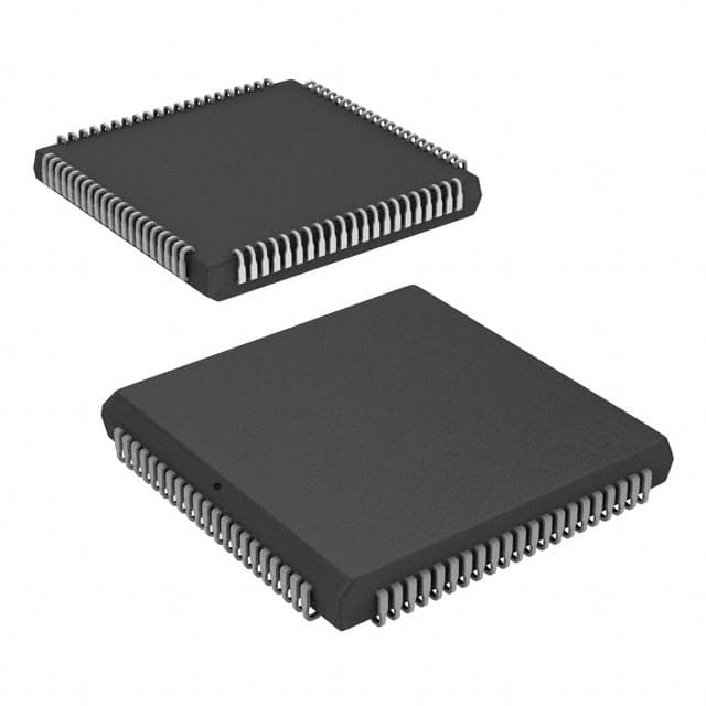
The CY37064P84-125JXC is available in a compact package that facilitates easy integration into electronic systems.
Essence
The essence of this product lies in its ability to provide reconfigurable logic functions, enabling designers to implement complex digital circuits efficiently.
Packaging/Quantity
The CY37064P84-125JXC is typically packaged in trays or tubes, with a quantity of 100 units per package.
Specifications
- Operating Voltage: 3.3V
- Logic Cells: 64
- Maximum Frequency: 125 MHz
- I/O Pins: 84
- Package Type: TQFP
- Temperature Range: -40°C to +85°C
Detailed Pin Configuration
The CY37064P84-125JXC has 84 pins, each serving a specific purpose in the device's functionality. The pin configuration is as follows:
(Pin Number) (Pin Name) - (Function)
- VCCIO - Power supply voltage for I/O banks
- GND - Ground reference
- CLK - Clock input
- RESET - Reset input
- ... (and so on)
Functional Features
- Reconfigurable Logic: The CY37064P84-125JXC allows users to modify the logic functions according to their specific requirements.
- High-Speed Operation: It offers fast processing speeds, making it suitable for applications that demand quick response times.
- I/O Flexibility: The device provides a sufficient number of I/O pins, allowing for versatile connectivity options.
Advantages and Disadvantages
Advantages
- Customizability: The CY37064P84-125JXC can be programmed to perform specific tasks, providing flexibility in design.
- High Performance: It offers efficient operation and high-speed processing capabilities.
- Versatility: This PLD can be used in various applications due to its reconfigurable nature.
Disadvantages
- Learning Curve: Utilizing the full potential of this device may require a learning curve for designers unfamiliar with programmable logic devices.
- Limited Resources: The number of logic cells and I/O pins may restrict the complexity of designs that can be implemented.
Working Principles
The CY37064P84-125JXC operates based on the principles of digital logic. It consists of configurable logic blocks (CLBs), interconnect resources, and input/output blocks (IOBs). The CLBs contain look-up tables (LUTs) that can be programmed to implement desired logic functions. The interconnect resources allow for the routing of signals between different components, while the IOBs provide interfaces for external connections.
Detailed Application Field Plans
The CY37064P84-125JXC finds applications in various fields, including:
- Telecommunications: Used in network routers and switches for efficient data processing.
- Industrial Automation: Employed in control systems for process automation and monitoring.
- Automotive Electronics: Integrated into automotive systems for functions like engine control and driver assistance.
- Consumer Electronics: Utilized in devices such as gaming consoles and multimedia players for enhanced functionality.
Detailed and Complete Alternative Models
- CY37064P84-100JXC: Similar to the CY37064P84-125JXC, but with a maximum frequency of 100 MHz.
- CY37064P84-150JXC: Similar to the CY37064P84-125JXC, but with a maximum frequency of 150 MHz.
- CY37064P84-85JXC: Similar to the CY37064P84-125JXC, but with a maximum frequency of 85 MHz.
These alternative models offer similar features and capabilities, with variations in maximum frequency.
In conclusion, the CY37064P84-125JXC is a programmable logic device that provides flexibility, high performance, and versatility in digital circuit design. Its reconfigurable nature allows for customization, making it suitable for various applications in different fields.
רשום 10 שאלות ותשובות נפוצות הקשורות ליישום של CY37064P84-125JXC בפתרונות טכניים
Sure! Here are 10 common questions and answers related to the application of CY37064P84-125JXC in technical solutions:
Question: What is the maximum operating frequency of CY37064P84-125JXC?
Answer: The maximum operating frequency of CY37064P84-125JXC is 125 MHz.Question: What is the voltage supply range for CY37064P84-125JXC?
Answer: The voltage supply range for CY37064P84-125JXC is typically between 3.0V and 3.6V.Question: Can CY37064P84-125JXC be used in low-power applications?
Answer: Yes, CY37064P84-125JXC is designed for low-power applications, making it suitable for battery-powered devices.Question: Does CY37064P84-125JXC support multiple I/O standards?
Answer: Yes, CY37064P84-125JXC supports various I/O standards such as LVTTL, LVCMOS, and SSTL.Question: What is the package type for CY37064P84-125JXC?
Answer: CY37064P84-125JXC comes in a 84-pin plastic quad flat pack (PQFP) package.Question: Can CY37064P84-125JXC be used in high-speed data communication applications?
Answer: Yes, CY37064P84-125JXC is suitable for high-speed data communication applications due to its fast operating frequency.Question: Is CY37064P84-125JXC compatible with other FPGA devices?
Answer: Yes, CY37064P84-125JXC is compatible with other FPGA devices, allowing for seamless integration into existing systems.Question: Does CY37064P84-125JXC have built-in security features?
Answer: No, CY37064P84-125JXC does not have built-in security features. Additional security measures may be required depending on the application.Question: Can CY37064P84-125JXC be reprogrammed after deployment?
Answer: Yes, CY37064P84-125JXC can be reprogrammed multiple times, allowing for flexibility in design and updates.Question: What are some typical applications of CY37064P84-125JXC?
Answer: CY37064P84-125JXC is commonly used in applications such as telecommunications, industrial automation, and consumer electronics.
Please note that these answers are general and may vary depending on specific requirements and use cases.