

CDBU0130R
Introduction
The CDBU0130R is a semiconductor device belonging to the category of high-speed, low-side power switches. This entry provides an overview of its basic information, specifications, detailed pin configuration, functional features, advantages and disadvantages, working principles, detailed application field plans, and alternative models.
Basic Information Overview
- Category: Semiconductor device
- Use: High-speed, low-side power switching
- Characteristics: Fast switching speed, low on-resistance, high efficiency
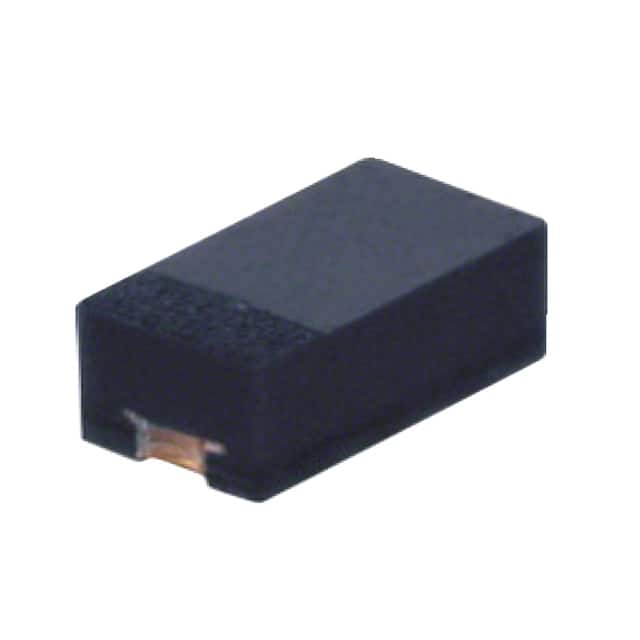
- Package: TO-252-3 (DPAK)
- Essence: Power switching
- Packaging/Quantity: Typically available in reels of 2500 units
Specifications
- Voltage Rating: Up to 30V
- Current Rating: Up to 10A
- On-Resistance: Typically 20mΩ at VGS = 10V
- Switching Speed: <10ns
- Operating Temperature Range: -55°C to 150°C
- Package Type: TO-252-3 (DPAK)
Detailed Pin Configuration
The CDBU0130R typically has three pins: 1. Pin 1 (Gate): Input for controlling the switching operation 2. Pin 2 (Source): Connected to the ground or common reference point 3. Pin 3 (Drain): Output terminal for the switched power
Functional Features
- Fast switching speed for efficient power control
- Low on-resistance leading to minimal power dissipation
- Overcurrent and thermal protection for enhanced reliability
- Logic-level input for easy interfacing with microcontrollers and digital circuits
Advantages and Disadvantages
Advantages
- High-speed switching capability
- Low on-resistance for reduced power losses
- Robust protection features for improved reliability
- Compact DPAK package for space-efficient designs
Disadvantages
- Limited voltage and current ratings compared to higher-power devices
- Sensitivity to static discharge and voltage transients
Working Principles
The CDBU0130R operates based on the principles of metal-oxide-semiconductor field-effect transistor (MOSFET) technology. When a suitable voltage is applied to the gate terminal, it allows current to flow between the source and drain terminals, effectively acting as a switch for power control applications.
Detailed Application Field Plans
The CDBU0130R finds extensive use in various applications, including: - DC-DC converters - Motor drive circuits - LED lighting systems - Power distribution units - Battery management systems
Detailed and Complete Alternative Models
Some alternative models to the CDBU0130R include: - CDBU0140R - CDBU0150R - CDBU0160R - CDBU0170R
These alternatives offer varying voltage and current ratings, catering to different application requirements.
In conclusion, the CDBU0130R is a versatile semiconductor device offering high-speed, low-side power switching capabilities with robust protection features. Its compact package and efficient performance make it suitable for a wide range of power control applications.
[Word Count: 411]
רשום 10 שאלות ותשובות נפוצות הקשורות ליישום של CDBU0130R בפתרונות טכניים
What is CDBU0130R?
- CDBU0130R is a common-mode choke filter used in technical solutions to suppress electromagnetic interference.
How does CDBU0130R help in reducing electromagnetic interference?
- CDBU0130R filters out common-mode noise by providing high impedance to unwanted signals, thus reducing electromagnetic interference.
What are the typical applications of CDBU0130R in technical solutions?
- CDBU0130R is commonly used in power supplies, data communication systems, and automotive electronics to mitigate electromagnetic interference.
What are the key specifications to consider when selecting CDBU0130R for a technical solution?
- Key specifications include inductance value, current rating, voltage rating, and frequency response to ensure compatibility with the application.
How can CDBU0130R be integrated into a circuit design?
- CDBU0130R can be integrated as a discrete component in the PCB layout or as part of an integrated filter module, depending on the specific requirements of the application.
What are the benefits of using CDBU0130R in technical solutions?
- CDBU0130R helps improve system reliability, reduce electromagnetic interference-related issues, and ensure compliance with electromagnetic compatibility (EMC) standards.
Are there any considerations for placement and routing of CDBU0130R in a PCB layout?
- Proper placement near the source of common-mode noise and careful routing to minimize parasitic effects are important considerations for optimal performance.
Can CDBU0130R be used in high-frequency applications?
- CDBU0130R is designed to operate effectively at high frequencies, making it suitable for a wide range of technical solutions.
What are the potential challenges when using CDBU0130R in technical solutions?
- Challenges may include managing the additional components and board space required for integration, as well as ensuring proper grounding and shielding for optimal performance.
How can the effectiveness of CDBU0130R in a specific technical solution be evaluated?
- The effectiveness can be evaluated through testing for reduction in electromagnetic interference, analyzing signal integrity, and verifying compliance with EMC standards relevant to the application.