

AD9250BCPZRL7-170
Product Overview
Category
AD9250BCPZRL7-170 belongs to the category of integrated circuits (ICs).
Use
It is primarily used for analog-to-digital conversion in various electronic systems.
Characteristics
- High-speed and high-resolution analog-to-digital conversion
- Low power consumption
- Small form factor
- Wide input voltage range
- Excellent signal-to-noise ratio
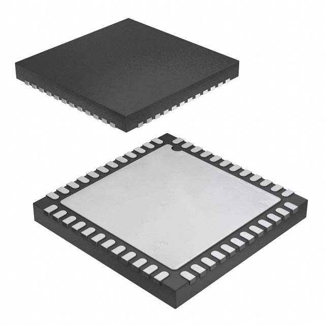
Package
AD9250BCPZRL7-170 comes in a compact package, which is suitable for surface mount technology (SMT) applications.
Essence
The essence of AD9250BCPZRL7-170 lies in its ability to convert analog signals into digital data with high precision and speed.
Packaging/Quantity
This product is typically packaged in reels or trays, with a quantity of 250 units per reel/tray.
Specifications
- Resolution: 12 bits
- Sampling Rate: 170 MSPS (Mega Samples Per Second)
- Input Voltage Range: ±1 V
- Power Supply: 3.3 V
- Operating Temperature Range: -40°C to +85°C
Detailed Pin Configuration
The pin configuration of AD9250BCPZRL7-170 is as follows:
- VDDA: Analog power supply
- VREF: Reference voltage input
- VIN: Analog input voltage
- GND: Ground
- CLK: Clock input
- D[11:0]: Digital output data
- CS: Chip select
- SCLK: Serial clock input
- RESET: Reset input
- DGND: Digital ground
Functional Features
- High-speed sampling and conversion
- Low power consumption
- Excellent linearity and dynamic range
- Built-in digital signal processing functions
- Flexible interface options (serial or parallel)
- Programmable gain and offset calibration
Advantages and Disadvantages
Advantages
- High-resolution conversion
- Wide input voltage range
- Low power consumption
- Compact form factor
- Excellent signal-to-noise ratio
Disadvantages
- Relatively high cost compared to lower-end ADCs
- Requires careful PCB layout and grounding for optimal performance
Working Principles
AD9250BCPZRL7-170 operates based on the principle of successive approximation. It samples the analog input voltage at a high rate, converts it into a digital representation, and outputs the result in binary format. The internal circuitry ensures accurate conversion by minimizing errors such as quantization noise and non-linearity.
Detailed Application Field Plans
AD9250BCPZRL7-170 finds applications in various fields, including:
- Communications: Used in wireless base stations, software-defined radios, and satellite communication systems.
- Test and Measurement: Employed in oscilloscopes, spectrum analyzers, and data acquisition systems.
- Medical Imaging: Integrated into ultrasound machines, MRI scanners, and medical diagnostic equipment.
- Industrial Automation: Utilized in control systems, robotics, and process monitoring devices.
- Defense and Aerospace: Applied in radar systems, avionics, and electronic warfare equipment.
Detailed and Complete Alternative Models
- AD9649BCPZ-250: 14-bit, 250 MSPS ADC with similar characteristics and package.
- AD9265BCPZ-80: 16-bit, 80 MSPS ADC with comparable features and pin configuration.
- AD9218BSTZ-40: 10-bit, 40 MSPS ADC suitable for lower-speed applications.
These alternative models offer different resolutions, sampling rates, and price points to cater to diverse application requirements.
In conclusion, AD9250BCPZRL7-170 is a high-performance analog-to-digital converter that offers excellent speed, resolution, and power efficiency. Its compact package and versatile features make it suitable for various applications in industries such as communications, test and measurement, medical imaging, industrial automation, defense, and aerospace.
רשום 10 שאלות ותשובות נפוצות הקשורות ליישום של AD9250BCPZRL7-170 בפתרונות טכניים
Sure! Here are 10 common questions and answers related to the application of AD9250BCPZRL7-170 in technical solutions:
Q: What is the AD9250BCPZRL7-170? A: The AD9250BCPZRL7-170 is a high-speed analog-to-digital converter (ADC) designed for applications that require high-resolution digitization of wideband signals.
Q: What is the maximum sampling rate of the AD9250BCPZRL7-170? A: The AD9250BCPZRL7-170 has a maximum sampling rate of 170 MSPS (Mega Samples Per Second).
Q: What is the resolution of the AD9250BCPZRL7-170? A: The AD9250BCPZRL7-170 has a resolution of 12 bits, meaning it can represent analog signals with 4096 discrete levels.
Q: What is the input voltage range of the AD9250BCPZRL7-170? A: The AD9250BCPZRL7-170 has a differential input voltage range of ±1 V.
Q: What is the power supply voltage required for the AD9250BCPZRL7-170? A: The AD9250BCPZRL7-170 requires a single power supply voltage of +1.8 V.
Q: What is the typical power consumption of the AD9250BCPZRL7-170? A: The AD9250BCPZRL7-170 typically consumes around 500 mW (milliwatts) of power.
Q: What interface does the AD9250BCPZRL7-170 support? A: The AD9250BCPZRL7-170 supports a serial LVDS (Low Voltage Differential Signaling) interface for data transfer.
Q: Can the AD9250BCPZRL7-170 be used in high-frequency applications? A: Yes, the AD9250BCPZRL7-170 is suitable for high-frequency applications as it has a wide bandwidth and fast sampling rate.
Q: What are some typical applications of the AD9250BCPZRL7-170? A: The AD9250BCPZRL7-170 is commonly used in radar systems, software-defined radios, medical imaging equipment, and other high-speed data acquisition systems.
Q: Is the AD9250BCPZRL7-170 available in a small form factor package? A: Yes, the AD9250BCPZRL7-170 is available in a compact 32-lead LFCSP (Lead Frame Chip Scale Package) for space-constrained designs.
Please note that these answers are general and may vary depending on specific application requirements and datasheet specifications.