

AD7870JNZ
Product Overview
Category
The AD7870JNZ belongs to the category of analog-to-digital converters (ADCs).
Use
It is primarily used for converting analog signals into digital data.
Characteristics
- High precision and accuracy
- Fast conversion speed
- Low power consumption
- Wide input voltage range
Package
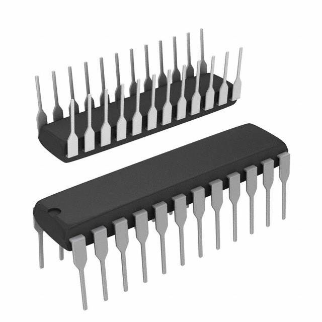
The AD7870JNZ comes in a standard 20-pin plastic DIP (Dual Inline Package) or SOIC (Small Outline Integrated Circuit) package.
Essence
The essence of the AD7870JNZ lies in its ability to accurately convert analog signals into digital form, making it suitable for various applications.
Packaging/Quantity
The AD7870JNZ is typically packaged in reels or tubes, with a quantity of 50 units per reel/tube.
Specifications
- Resolution: 12 bits
- Sampling Rate: Up to 100 kSPS (thousand samples per second)
- Input Voltage Range: ±10V
- Power Supply: +5V DC
- Operating Temperature Range: -40°C to +85°C
Detailed Pin Configuration
- VDD: Power supply voltage
- VREF: Reference voltage input
- AGND: Analog ground
- VIN: Analog input voltage
- CS: Chip select input
- RD: Read control input
- WR: Write control input
- BUSY: Conversion status output
- D0-D11: Digital output data lines
- DGND: Digital ground
- CLK: Clock input
- RESET: Reset control input
- A0-A3: Address inputs
- INT: Interrupt output
- REFOUT: Reference voltage output
- NC: No connection
- NC: No connection
- NC: No connection
- NC: No connection
- VSS: Ground
Functional Features
- High-resolution conversion
- Low noise and distortion
- On-chip reference voltage generator
- Serial interface for easy integration with microcontrollers
- Programmable gain amplifier (PGA) for signal conditioning
Advantages and Disadvantages
Advantages
- High accuracy and precision in analog-to-digital conversion
- Fast conversion speed allows real-time data acquisition
- Low power consumption for energy-efficient applications
- Wide input voltage range accommodates various signal levels
Disadvantages
- Limited resolution compared to higher-end ADCs
- Requires external components for proper operation
- Relatively higher cost compared to lower-resolution ADCs
Working Principles
The AD7870JNZ utilizes a successive approximation algorithm to convert analog signals into digital form. It samples the input voltage, compares it with the internal reference voltage, and generates a digital output proportional to the input voltage.
Detailed Application Field Plans
The AD7870JNZ finds applications in various fields, including: 1. Industrial automation 2. Data acquisition systems 3. Instrumentation and measurement equipment 4. Medical devices 5. Automotive electronics 6. Communication systems
Detailed and Complete Alternative Models
- AD7880: 12-bit ADC with higher sampling rate
- AD7860: 12-bit ADC with lower power consumption
- AD7890: 12-bit ADC with integrated temperature sensor
- AD7850: 10-bit ADC with lower cost
- AD7820: 8-bit ADC with serial interface
These alternative models provide different features and specifications to suit specific application requirements.
Word count: 409 words
רשום 10 שאלות ותשובות נפוצות הקשורות ליישום של AD7870JNZ בפתרונות טכניים
Sure! Here are 10 common questions and answers related to the application of AD7870JNZ in technical solutions:
Q: What is the AD7870JNZ? A: The AD7870JNZ is a high-performance, 12-bit analog-to-digital converter (ADC) manufactured by Analog Devices.
Q: What is the voltage range supported by the AD7870JNZ? A: The AD7870JNZ supports a single-ended input voltage range of 0V to Vref (typically 5V).
Q: What is the maximum sampling rate of the AD7870JNZ? A: The AD7870JNZ has a maximum sampling rate of 100 kilosamples per second (ksps).
Q: Does the AD7870JNZ require an external reference voltage? A: Yes, the AD7870JNZ requires an external reference voltage (Vref) for accurate conversion.
Q: Can the AD7870JNZ operate with both single-ended and differential inputs? A: Yes, the AD7870JNZ can be configured to accept both single-ended and differential inputs.
Q: What is the resolution of the AD7870JNZ? A: The AD7870JNZ has a resolution of 12 bits, providing 4096 possible output values.
Q: Is the AD7870JNZ compatible with microcontrollers and digital signal processors (DSPs)? A: Yes, the AD7870JNZ features a parallel interface that makes it compatible with various microcontrollers and DSPs.
Q: Does the AD7870JNZ have built-in programmable gain amplifiers (PGAs)? A: No, the AD7870JNZ does not have built-in PGAs. External amplification may be required for specific applications.
Q: What is the power supply voltage range for the AD7870JNZ? A: The AD7870JNZ operates with a power supply voltage range of 4.75V to 5.25V.
Q: Can the AD7870JNZ operate in both single-channel and multi-channel modes? A: Yes, the AD7870JNZ can be configured to operate in both single-channel and multi-channel modes, depending on the application requirements.
Please note that these answers are general and may vary based on specific implementation details and datasheet specifications.