

AD7391AN
Product Overview
Category
AD7391AN belongs to the category of digital-to-analog converters (DACs).
Use
The AD7391AN is used to convert digital signals into analog voltage outputs.
Characteristics
- High resolution and accuracy
- Low power consumption
- Wide operating temperature range
- Small package size
- Easy integration with microcontrollers
Package
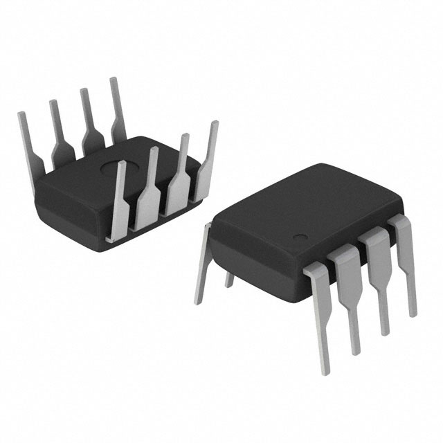
AD7391AN is available in a 16-pin plastic dual in-line package (PDIP).
Essence
The essence of AD7391AN lies in its ability to provide precise analog voltage outputs based on digital input signals.
Packaging/Quantity
AD7391AN is typically packaged in reels, with 1000 units per reel.
Specifications
- Resolution: 12 bits
- Supply Voltage Range: 2.7V to 5.5V
- Operating Temperature Range: -40°C to +85°C
- Output Voltage Range: 0V to Vref
- Reference Voltage: Internal or external reference options
- Power Consumption: Low power operation, typically 0.5mW
Detailed Pin Configuration
The AD7391AN has a total of 16 pins, which are assigned specific functions as follows:
- VDD: Positive supply voltage
- VSS: Ground
- REF IN: External reference voltage input
- AGND: Analog ground
- VOUT: Analog output voltage
- DB11: Digital input bit 11
- DB10: Digital input bit 10
- DB9: Digital input bit 9
- DB8: Digital input bit 8
- DB7: Digital input bit 7
- DB6: Digital input bit 6
- DB5: Digital input bit 5
- DB4: Digital input bit 4
- DB3: Digital input bit 3
- DB2: Digital input bit 2
- DB1: Digital input bit 1
Functional Features
- High-resolution digital-to-analog conversion
- Fast settling time for accurate voltage outputs
- Low power consumption for energy-efficient operation
- Flexible reference voltage options for versatile applications
- Easy integration with microcontrollers and other digital systems
Advantages and Disadvantages
Advantages
- High resolution and accuracy ensure precise analog voltage outputs.
- Low power consumption makes it suitable for battery-powered devices.
- Wide operating temperature range allows for use in various environments.
- Small package size enables space-saving designs.
- Easy integration with microcontrollers simplifies system implementation.
Disadvantages
- Limited output voltage range may not be suitable for certain applications requiring higher voltages.
- External reference voltage may be required for specific use cases, adding complexity to the design.
Working Principles
The AD7391AN operates based on the principle of digital-to-analog conversion. It takes digital input signals and converts them into corresponding analog voltage outputs. The internal circuitry of the DAC processes the digital data and generates an accurate analog voltage based on the applied reference voltage. This analog voltage can then be utilized in various applications that require precise control over analog signals.
Detailed Application Field Plans
The AD7391AN finds applications in a wide range of fields, including:
- Industrial automation: Control systems requiring accurate analog voltage outputs.
- Test and measurement equipment: Generating precise analog signals for testing purposes.
- Audio equipment: Producing high-quality audio signals with low distortion.
- Instrumentation: Providing analog voltage references for sensors and transducers.
- Communication systems: Generating analog signals for modulation and demodulation processes.
Detailed and Complete Alternative Models
- AD7303: 8-bit digital-to-analog converter with similar features and performance.
- AD5621: 12-bit digital-to-analog converter with a different package option.
- AD5755: 16-bit digital-to-analog converter with enhanced resolution and accuracy.
These alternative models offer similar functionality to the AD7391AN and can be considered based on specific application requirements.
Word count: 536 words
רשום 10 שאלות ותשובות נפוצות הקשורות ליישום של AD7391AN בפתרונות טכניים
Sure! Here are 10 common questions and answers related to the application of AD7391AN in technical solutions:
1. What is the AD7391AN? - The AD7391AN is a digital-to-analog converter (DAC) chip manufactured by Analog Devices.
2. What is the resolution of the AD7391AN? - The AD7391AN has a resolution of 12 bits, meaning it can convert digital input values into analog output voltages with a precision of 1 part in 4096.
3. What is the operating voltage range of the AD7391AN? - The AD7391AN operates from a single power supply voltage ranging from 2.7V to 5.5V.
4. What is the output voltage range of the AD7391AN? - The AD7391AN can generate an output voltage range of 0V to Vref, where Vref is the reference voltage supplied to the chip.
5. How does the AD7391AN communicate with a microcontroller or other digital devices? - The AD7391AN uses a serial interface called SPI (Serial Peripheral Interface) to communicate with external devices.
6. Can the AD7391AN be used for both unipolar and bipolar applications? - Yes, the AD7391AN can be configured for both unipolar (0V to Vref) and bipolar (-Vref/2 to +Vref/2) applications.
7. What is the settling time of the AD7391AN? - The settling time of the AD7391AN is typically 4 μs, which refers to the time it takes for the output voltage to reach within a specified error band after a change in the digital input.
8. Does the AD7391AN have any built-in reference voltage? - No, the AD7391AN requires an external reference voltage to generate the analog output. The reference voltage should be within the operating voltage range of the chip.
9. Can multiple AD7391AN chips be daisy-chained together? - Yes, multiple AD7391AN chips can be daisy-chained together using the SPI interface, allowing for simultaneous control of multiple DACs.
10. What are some typical applications of the AD7391AN? - The AD7391AN is commonly used in various applications such as industrial process control, instrumentation, data acquisition systems, programmable logic controllers (PLCs), and audio equipment.
Please note that these answers are general and may vary depending on specific implementation details and requirements.