

AD664JN-UNI
Product Overview
Category
AD664JN-UNI belongs to the category of integrated circuits (ICs).
Use
This product is commonly used in electronic devices for analog-to-digital conversion.
Characteristics
- High precision and accuracy
- Fast conversion speed
- Low power consumption
- Wide operating voltage range
Package
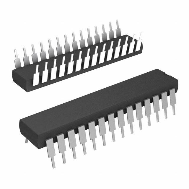
AD664JN-UNI is available in a standard dual in-line package (DIP).
Essence
The essence of AD664JN-UNI lies in its ability to convert analog signals into digital data with high fidelity.
Packaging/Quantity
This product is typically packaged in reels or tubes, with quantities varying based on customer requirements.
Specifications
- Resolution: 12 bits
- Sampling Rate: 1 MSPS (Million Samples Per Second)
- Input Voltage Range: ±10V
- Power Supply: +5V
- Operating Temperature Range: -40°C to +85°C
Detailed Pin Configuration
AD664JN-UNI has a total of 28 pins. The pin configuration is as follows:
- VREF-
- VREF+
- AGND
- VIN-
- VIN+
- DGND
- D0
- D1
- D2
- D3
- D4
- D5
- D6
- D7
- D8
- D9
- D10
- D11
- CS
- WR
- RD
- A0
- A1
- A2
- A3
- A4
- A5
- VCC
Functional Features
- High-speed parallel interface for efficient data transfer
- On-chip sample-and-hold circuitry for accurate conversion
- Built-in reference voltage generator for simplified design
- Power-down mode for reduced power consumption during idle periods
Advantages and Disadvantages
Advantages
- High precision and accuracy in analog-to-digital conversion
- Fast conversion speed enables real-time data processing
- Low power consumption for energy-efficient operation
- Wide operating voltage range allows for versatile applications
Disadvantages
- Limited resolution compared to higher-end models
- Higher cost compared to lower-resolution alternatives
- Requires external components for proper operation
Working Principles
AD664JN-UNI utilizes a successive approximation technique to convert analog signals into digital data. The input voltage is sampled, held, and compared against a reference voltage. The converter iteratively adjusts the digital output until it matches the input voltage within the specified resolution.
Detailed Application Field Plans
AD664JN-UNI finds applications in various fields, including: 1. Industrial automation 2. Data acquisition systems 3. Medical instrumentation 4. Communication equipment 5. Test and measurement devices
Detailed and Complete Alternative Models
- AD662JN-UNI: 10-bit resolution, 500 kSPS sampling rate
- AD666JN-UNI: 14-bit resolution, 2 MSPS sampling rate
- AD668JN-UNI: 16-bit resolution, 1 MSPS sampling rate
- AD672JN-UNI: 8-bit resolution, 1 MSPS sampling rate
These alternative models offer different resolutions and sampling rates to cater to specific application requirements.
In conclusion, AD664JN-UNI is a high-performance analog-to-digital converter with 12-bit resolution and a sampling rate of 1 MSPS. It offers high precision, fast conversion speed, and low power consumption. While it has certain limitations, such as limited resolution and higher cost, it is widely used in various fields for accurate signal conversion.
רשום 10 שאלות ותשובות נפוצות הקשורות ליישום של AD664JN-UNI בפתרונות טכניים
Sure! Here are 10 common questions and answers related to the application of AD664JN-UNI in technical solutions:
Question: What is the AD664JN-UNI?
Answer: The AD664JN-UNI is a high-performance, 12-bit analog-to-digital converter (ADC) manufactured by Analog Devices.Question: What is the maximum sampling rate of the AD664JN-UNI?
Answer: The AD664JN-UNI has a maximum sampling rate of 100 kilosamples per second (ksps).Question: What is the resolution of the AD664JN-UNI?
Answer: The AD664JN-UNI has a resolution of 12 bits, which means it can represent analog signals with 4096 discrete levels.Question: What is the input voltage range of the AD664JN-UNI?
Answer: The AD664JN-UNI has a bipolar input voltage range of ±10 volts.Question: Can the AD664JN-UNI be used in single-ended mode?
Answer: No, the AD664JN-UNI is a differential ADC and requires differential input signals.Question: What is the power supply voltage range for the AD664JN-UNI?
Answer: The AD664JN-UNI operates from a single power supply voltage ranging from +5 volts to +15 volts.Question: Does the AD664JN-UNI have built-in digital signal processing features?
Answer: No, the AD664JN-UNI is a standalone ADC and does not have built-in digital signal processing capabilities.Question: What is the typical power consumption of the AD664JN-UNI?
Answer: The typical power consumption of the AD664JN-UNI is 100 milliwatts (mW).Question: Can the AD664JN-UNI be used in industrial applications?
Answer: Yes, the AD664JN-UNI is suitable for a wide range of industrial applications, including process control and instrumentation.Question: What are some common interface options for connecting the AD664JN-UNI to a microcontroller or FPGA?
Answer: Common interface options include parallel interfaces such as parallel data bus or multiplexed address/data bus, as well as serial interfaces like SPI (Serial Peripheral Interface) or I2C (Inter-Integrated Circuit).