

AD5361BSTZ
Basic Information Overview
- Category: Integrated Circuit (IC)
- Use: Digital-to-Analog Converter (DAC)
- Characteristics:
- High resolution and accuracy
- Low power consumption
- Small package size
- Wide operating temperature range
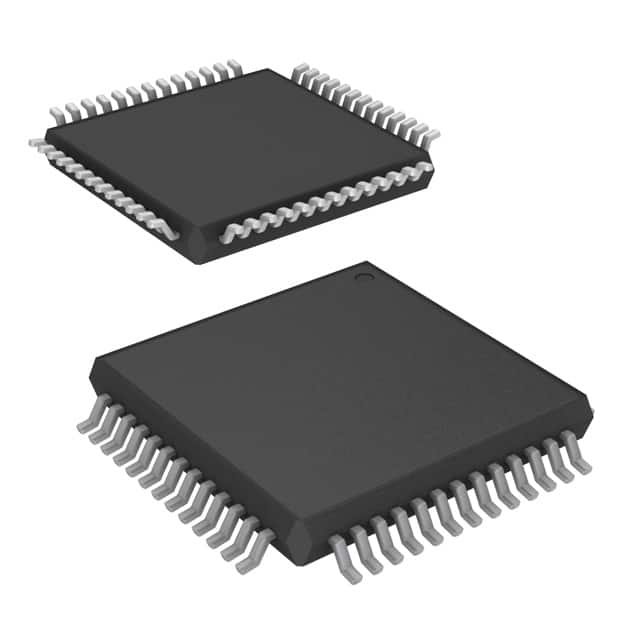
- Package: BSTZ (Thin Shrink Small Outline Package)
- Essence: AD5361BSTZ is a high-performance DAC designed for various applications.
- Packaging/Quantity: Available in tape and reel packaging, with a quantity of 2500 units per reel.
Specifications
- Resolution: 16 bits
- Number of Channels: 1
- Output Type: Voltage
- Supply Voltage: 2.7V to 5.5V
- Operating Temperature Range: -40°C to +105°C
- Interface: Serial Peripheral Interface (SPI)
Detailed Pin Configuration
The AD5361BSTZ has the following pin configuration:
| Pin Name | Description | |----------|-------------| | VDD | Power supply voltage | | GND | Ground reference | | DIN | Serial data input | | SCLK | Serial clock input | | SYNC | Chip select input | | VOUT | Analog output voltage |
Functional Features
- High-resolution digital-to-analog conversion
- Low power consumption for energy-efficient operation
- SPI interface for easy integration with microcontrollers
- Internal reference voltage for improved accuracy
- Programmable output voltage range
- Power-on reset function for reliable startup
Advantages
- High resolution and accuracy enable precise analog signal generation.
- Low power consumption makes it suitable for battery-powered devices.
- Small package size allows for space-constrained designs.
- Wide operating temperature range ensures reliable performance in various environments.
Disadvantages
- Limited to single-channel output.
- Requires an external microcontroller or control circuitry for operation.
- Higher cost compared to lower-resolution DACs.
Working Principles
The AD5361BSTZ utilizes a digital-to-analog conversion technique to convert binary input data into an analog voltage output. The internal circuitry of the IC processes the serial input data and generates the corresponding analog voltage based on the resolution and reference voltage settings. The SPI interface facilitates communication with an external microcontroller or control system, allowing for precise control over the output voltage.
Detailed Application Field Plans
The AD5361BSTZ is widely used in various applications that require accurate analog voltage generation. Some of the key application fields include: - Industrial automation and control systems - Test and measurement equipment - Audio and video signal processing - Instrumentation and data acquisition systems - Communication infrastructure
Detailed and Complete Alternative Models
- AD5360: 16-bit, single-channel DAC with similar features but different package options.
- AD5362: 16-bit, dual-channel DAC for applications requiring multiple outputs.
- AD5364: 16-bit, quad-channel DAC offering increased channel density.
These alternative models provide flexibility in terms of channel count and package options, catering to different design requirements.
Word Count: 334 words
רשום 10 שאלות ותשובות נפוצות הקשורות ליישום של AD5361BSTZ בפתרונות טכניים
Sure! Here are 10 common questions and answers related to the application of AD5361BSTZ:
Q1: What is AD5361BSTZ? A1: AD5361BSTZ is a specific model of the AD5361 family of digital-to-analog converters (DACs) manufactured by Analog Devices.
Q2: What is the resolution of AD5361BSTZ? A2: AD5361BSTZ has a resolution of 16 bits, meaning it can provide 2^16 (65,536) different output voltage levels.
Q3: What is the operating voltage range of AD5361BSTZ? A3: AD5361BSTZ operates with a single supply voltage ranging from 2.7V to 5.5V.
Q4: How many channels does AD5361BSTZ have? A4: AD5361BSTZ has 8 independent channels, allowing for simultaneous control of multiple outputs.
Q5: What is the maximum output voltage range of AD5361BSTZ? A5: The output voltage range of AD5361BSTZ is programmable and can be set between 0V and VREF (the reference voltage).
Q6: Can AD5361BSTZ operate in both unipolar and bipolar modes? A6: Yes, AD5361BSTZ can be configured to operate in either unipolar or bipolar mode, depending on the application requirements.
Q7: What is the settling time of AD5361BSTZ? A7: The settling time of AD5361BSTZ is typically around 10 μs, ensuring fast and accurate voltage output transitions.
Q8: Does AD5361BSTZ support serial communication interfaces? A8: Yes, AD5361BSTZ supports various serial communication interfaces such as SPI (Serial Peripheral Interface) and I2C (Inter-Integrated Circuit).
Q9: Can AD5361BSTZ be used in precision measurement applications? A9: Yes, AD5361BSTZ is suitable for precision measurement applications due to its high resolution and low integral nonlinearity.
Q10: What are some typical applications of AD5361BSTZ? A10: AD5361BSTZ can be used in various applications such as industrial automation, process control, motor control, audio equipment, and instrumentation.
Please note that these answers are general and may vary depending on the specific requirements and use cases.